
Via in Pad
As miniaturisation of electronics continues via holes in pads are seen as a solution to gain more real estate on PCB’s. However, when used incorrectly, a via in pad can cause a variety of soldering issues which can reduce the quality of your final product.
The primary issue with via in pad is that if the hole is not filled or capped correctly, solder will wick into it during the reflow process and may leave the pad with insufficient solder. This can lead to poor thermal and electrical performance. In addition, voids can form in the via which can affect the strength and reliability of the connection.
One way to prevent solder wicking in a via is to use Kapton tape. The kapton will cover the uncapped via and stop it from wicking solder during reflow. However, this is a temporary solution and should not be relied upon. Another way to prevent solder wicking is to cover the pad and any large area or via connected to it with solder mask. This will prevent the solder from wicking into these areas and will allow it to stay on the pads.
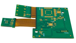
Soldering Issues With a Via in Pad
The last method to prevent soldering issues with a via in pad is to limit the number of these types of holes on the board and only place them where it is absolutely necessary. This will help to reduce manufacturing complexity and costs. If you must have a via in pad on your circuit board, it is recommended that you stick to the recommendations from the component manufacturer for pad and via size, capping and filling.
A further issue with via in pads is that if they are left open then the copper will be exposed to the environment, which can result in oxidation and shorten the PCB life. This can be avoided by ensuring that the pad size on the board is larger than the via and IPC annular ring sizes. It is also advisable to use Solder Mask Defined pads where possible so that you can guarantee the pad size is correct.
If the ring surrounding a via is not adequately filled and capped then it can be difficult to place a BGA ball over it. This is because the solder in the ring will not have enough continuity to join with the solder on the ball. The best solution is to ensure that the ring surrounding the via is fully filled with an epoxy resin and then plated over before using the pad on the board.
It is also important to be aware of the fact that the ring surrounding the via can be damaged by vibration and mechanical stress. This can result in a loose or broken solder joint which is prone to failure under environmental conditions such as high temperature and vibration. To avoid this, the ring around the via should be carefully designed with a good thermal path and be able to dissipate heat effectively.